Samsung galaxy s3 circuit diagram pdf Galaxy s3 circuit board diagram Motherboard 4g ic mainboard bluetooth broadcom 3g
Samsung S3 Circuit Board Diagram
Samsung s3 circuit board diagram
S4 diagram galaxy motherboard samsung pcb saved wordpress circuit
Unlocking the secrets: samsung s4 schematic diagram revealedSamsung galaxy s3 circuit board diagram Samsung galaxy teardown circuit technologies splitting mm ii latest global main boardGalaxy s4 circuit diagram.
Samsung galaxy schematics s3Samsung s3 schematic diagram I9300 schematics galaxy tháng sáu pham haiGalaxy s schematics.
![Samsung S3 Circuit Board Diagram](https://i2.wp.com/sc01.alicdn.com/kf/HTB1CQGNKFXXXXagXVXXq6xXFXXXl/CRT-TV-main-board-for-14-inch.jpg)
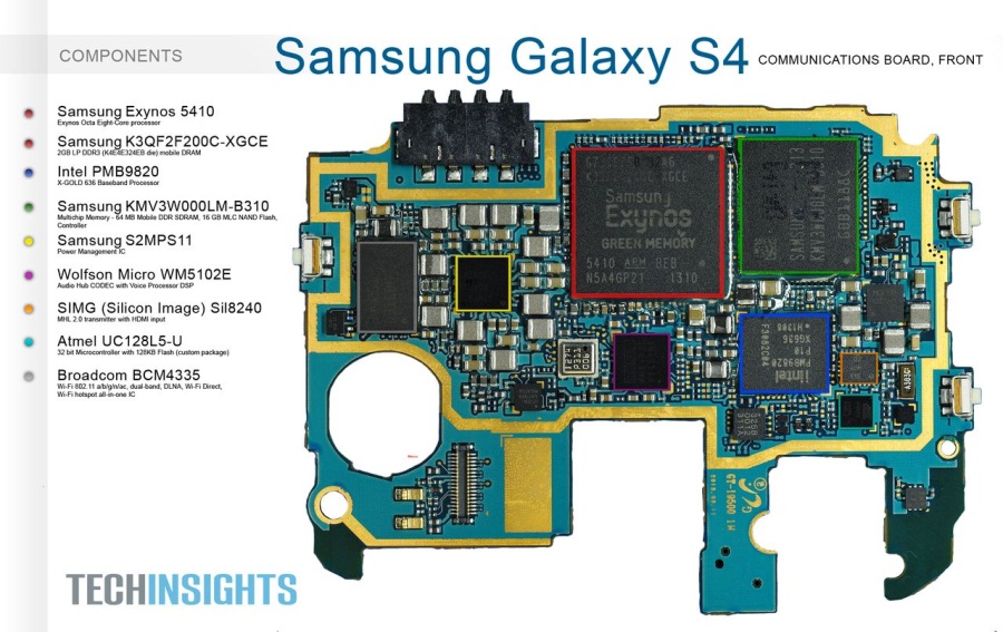
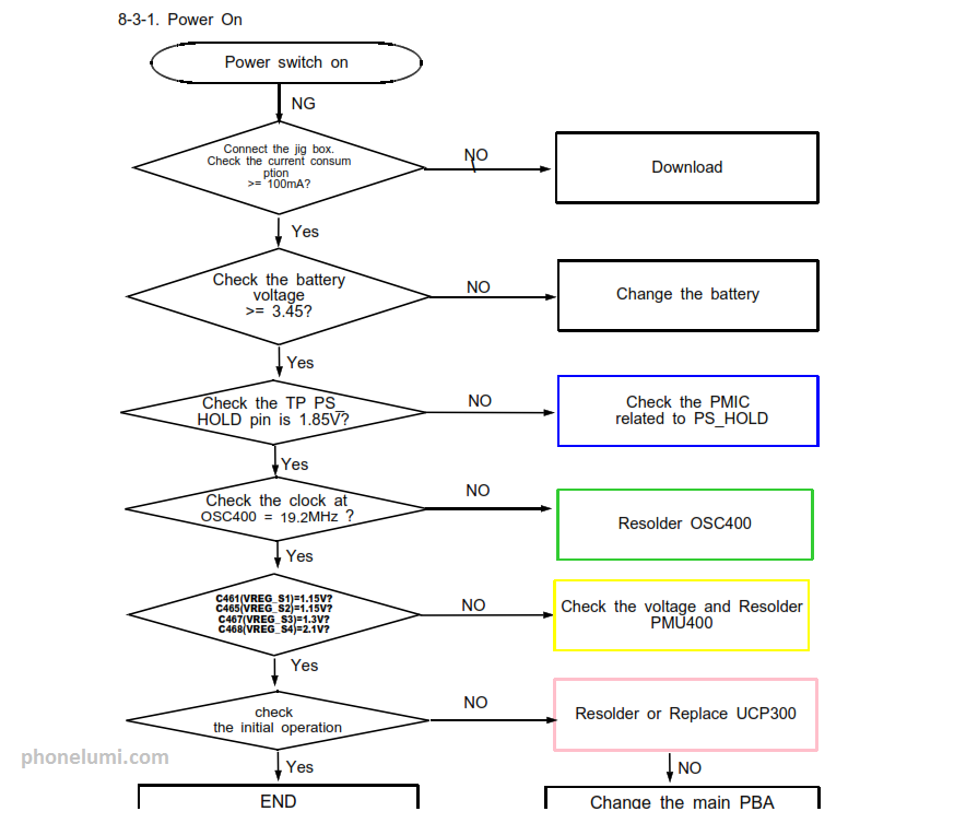
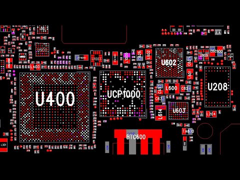
Schematic diagram of samsung galaxy s4
Samsung s3 circuit board diagramSamsung j2 prime schematic diagram pdf Samsung s3 schematic diagramGalaxy s3 circuit board diagram.
Samsung s3 circuit board diagramGalaxy s3 circuit board diagram Galaxy s3 circuit board diagramSamsung galaxy s 4g pcb board components layout ~ mobile phone repair.
![Galaxy S II Teardown – Splitting 8.9 mm of the latest Samsung](https://i2.wp.com/img.global.news.samsung.com/global/wp-content/uploads/2011/07/9.jpg)
Samsung galaxy s3 i9300 schematics
Galaxy s ii teardown – splitting 8.9 mm of the latest samsungSamsung s3 circuit board diagram Samsung s3 circuit board diagramSamsung schematic diagram.
Samsung i9500 galaxy s4 charging jumper3/1/11 ~ mobile phone repair guides Samsung galaxy s4 circuit diagramGalaxy s3 circuit board diagram.
![microcontroller - Connecting power to ground through a capacitor in](https://i2.wp.com/i.stack.imgur.com/aDnhJ.png)
Schematic i9300 gt galaxy s4 pcb s5 samsung i9500
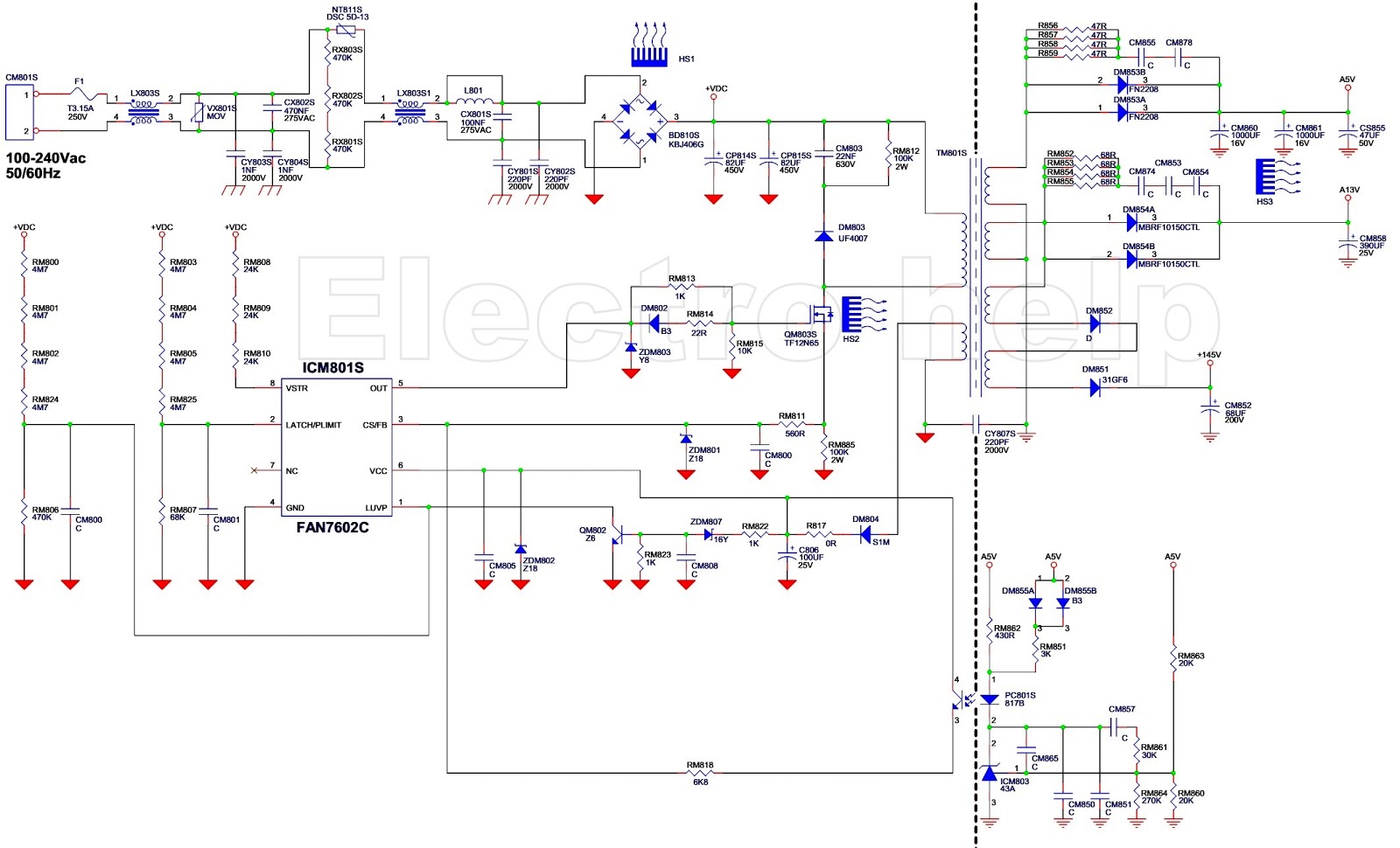
Samsung galaxy s5 circuit diagramSamsung tv circuit board diagram un55ks800df Samsung galaxy s3 circuit diagram pdfGt-i9300 galaxy s3 pcb schematic.
Samsung crt tv circuit board diagramSamsung board galaxy pcb mobile layout 4g Top pcb.
![Galaxy S3 Circuit Board Diagram](https://1.bp.blogspot.com/-5cDmc1lOHME/UYPeaeMNVYI/AAAAAAAAAJQ/5ZyJ2bm4sw0/s1600/samsung+Galaxys4.jpg)
![Samsung Galaxy S3 Circuit Diagram Pdf](https://3.bp.blogspot.com/-ojH4EuPrl6s/V7uWj2reHCI/AAAAAAAARFY/JdpVUvb8rUg1Zeo1PJTYyMKuaeBLWsaRgCLcB/s1600/samsung%2Bi9300i%2Bschematics1.png)
![GT-I9300 Galaxy S3 pcb schematic - YouTube](https://i.ytimg.com/vi/cANVmBwhZjw/hqdefault.jpg)
![Samsung Galaxy S3 Circuit Board Diagram](https://i.pinimg.com/originals/df/53/4e/df534e139d72b8100b8abd36d379916a.png)
![Galaxy S Schematics - Cell Schematics & Service Manual PDF](https://i2.wp.com/image.jimcdn.com/app/cms/image/transf/none/path/s9561acb0f0916d6e/image/ib44a18627c2e45ba/version/1552166040/samsung-galaxy-s3-schematics.jpg)
![Samsung S3 Circuit Board Diagram](https://1.bp.blogspot.com/-vDOk-mVnxGc/VekrfIup2PI/AAAAAAABNpQ/_OnEOQ8ULSQ/s1600/SCHEMATIC-1.jpg)
![Samsung I9500 Galaxy S4 Charging Jumper](https://2.bp.blogspot.com/-Wx8vfLli11Q/VGz5OXp5R_I/AAAAAAAAAzI/5hd8a4rzdpY/s1600/Samsung-I9500-Galaxy-S4-Charging-Solution-Jumper-Problem-Ways-Charging-Not-Supported.jpg)
![Galaxy S3 Circuit Board Diagram](https://i2.wp.com/img.gem-flash.com/images/34741113483825939052.jpg)
![Samsung Ua32f5100ar Circuit Diagram](https://1.bp.blogspot.com/-ToLC06ASFCE/WAzgmUQCS7I/AAAAAAABajM/K4OG9hON4PgWXcwYl_45kJHAKxfl8jfbACLcB/s1600/smps%2Band%2Bdeflection.jpg)